CIQM Research Areas
|
Research Area 1: Novel van der Waals Heterostructures
Coordinator Philip Kim By stacking 2D quantum materials, one can create atomic-scale heterostructures with a wide variety of properties. The layers can have different properties: graphene is a conductor, hBN is an insulator, and TMD materials such as MoS2 and WSe2 can be semiconductors or optoelectronic materials. By rotating the crystal axes as the atomic layers are stacked, twistronic heterostructures with Moire-pattern lattices can be formed. Van der Waals heterostructures have promise as sensors and devices in quantum systems. Research Area 2: Discovery of New Topological Crystals Coordinator: Joseph Checkelsky The topological insulator field began following an original theoretical prediction by Kane and Fu. At MIT, Fu has extended the frontier by inventing new classes of topological crystals. Through theoretical work by Aspuru-Guzik, growth by Checkelsky and Moodera, and characterization by Bell and other participants we plan to create new classes of topological crystals with theoretically predicted properties. Research Area 3: Topologically Protected Qubits
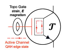
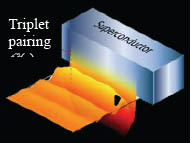
Coordinator: Amir Yacoby and Pablo Jarillo-Herrero A barrier to implementing quantum computers is incoherence from external perturbations. Topologically protected qubits are insensitive to external noise, so they bypass this obstacle. Fu predicted that Majorana fermions can be created in topological superconductors, to create a topologically robust qubit. Our Center plans to demonstrate the existence of Majorana's and to devise ways to braid them for quantum computation. Research Area 4: Quantum Networks with Engineered Solid State Quantum Emitters
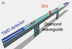
Coordinator: Marko Loncar Atomic-scale color centers in diamond provide a solid-state platform for the realization of scalable quantum networks that could link quantum computing stations at different locations thus realizing unprecedented distributed computational resource – a quantum cloud. To enable this, it is necessary to: i) engineer the emission rate and spectrum of quantum emitters, ii) improve the in- and out-coupling efficiency between emitted photons and the collection optics, iii) enable on-demand control the spin-state and iv) extend the coherence time of the spin memory. These tasks can be achieved by embedding quantum emitters in optical nanocavities and waveguides, and by using TMD to implement electro-optic I/O circuits. |


