|
Vision - Extraordinary new quantum materials enable atomic-scale electronics and photonics that transform signal processing and computation
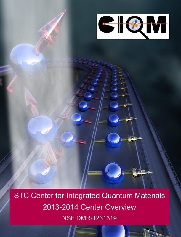
MIssion · Quantum materials will allow electronics and photonics to pass beyond the limits of conventional semiconductors. Atomic-layer materials such as graphene enable ultrafast devices, topological insulators give error-free data channels, and nitrogen vacancy (NV) centers in diamond form atomic memory sites and sensors. · Our Center will attract young students to careers in Science, Technology, Engineering, and Mathematics (STEM). · Our Center will have the gender and racial balance of our country. · Our Center's Education and Public Outreach Programs will engage young students and public audiences in the quest for new frontiers. · Our Center's Knowledge Transfer Program will commercialize research on quantum materials and devices into new products and technologies. Quantum Materials In the past decade, quantum materials have been discovered that have extraordinary properties for signal processing and computation systems: Atomic Layer Materials - Graphene (G), hexagonal boron nitride (BN), molybdenum disulfide (MoS2), and other atomic layer materials, are only a single atom or molecule thick. Graphene has no energy gap, and electrons move at a constant speed ~ 108 cm/sec; BN is an insulator, and MoS2 is semiconductor. These materials are natural for ultrafast, atomic-scale devices. Topological Insulators (TIs) - Bismuth selenide (Bi2Se3) and other topological insulators have conducting edge and surface states that topologically protect data by locking the direction of an electron's spin perpendicular to its momentum. TI materials are natural for protected data channels. Nitrogen Vacancy (NV) Centers in Diamond - The electron spin on an NV center can hold a qubit of information for > 1 ms at room temperature, to act as a one-atom memory site. Data is optically programmed and read out. In addition, an NV center forms an ultrasensitive, high spatial resolution magnetometer, capable of imaging the field of a single electron spin at room temperature. These materials offer quantum approaches to atomic-scale electronics and photonics based on their extraordinary quantum properties. By integrating Atomic Layer devices with Topological Insulator data channels, and NV Center sensors and memory, our Center plans to build new types of Quantum Electronic and Photonic Systems and Quantum Networks. |
Click to view
Bob Westervelt's CIQM Overview |
- About
-
News & Events
- Calendars
- News
-
Events
>
- FQMD 2022
- Site Visit 2022
- 2021 Annual Meeting
- 2020 STC Directors Meeting
- 2020 Tohoku Workshop
- 2019 Annual Meeting
- FQMD 2019 Frontiers in Quantum Materials and Devices
- Quantum Matters Competition >
- 2018 Annual Meeting
- 2017 Annual Meeting
- FQMD 2018 Frontiers in Quantum Materials and Devices
- FQMD 2017 Frontiers in Quantum Materials and Devices
- Retreat 2016 >
- Frontiers in Quantum Materials and Devices Workshop 2016
- Frontiers in Quantum Materials and Devices Workshop 2015 >
- Annual Meeting 2016 >
- Annual Meeting 2015 >
- Annual Meeting 2014 >
- Highlights
- Online Community
-
Education
- Research
- Knowledge Transfer
- Resources


